
“There are 2 ways to learn antenna design. One way is to go to grad school. I’ll teach you the other way”
-A mentor of mine
Engineers love to refer to wireless as ‘black magic’. Which is partly true. But with the right tools and the willingness to fuck it all up (a few times), you’ll be making your mark on the 2.4GHz band in no time. This guide is a ‘Trial and Error’ approach to antenna design. It won’t be perfect, and won’t cover a lot of the ‘hard’ topics. You probably won’t even feel smart after reading it. You may even feel a little dirty. But you WILL be able to design an antenna to ‘good enough’ standards, for 2.4GHz communication (wifi, zigbee, ANT+, etc).
The basic procedure looks like this:
- Pick an IC
- Look at the Datasheet of your chip, find the example layout section
- Does your application have physical size limitations? Does your Antenna have to be directional?
- Use the answers to the above questions to choose your antenna type (whip, wire, chip, PCB trace)
- Design your PCB layout based on the example layout. Size the feedline for your application
- Build some boards
- Test the antenna with an SMA connector and a spectrum analyzer, if possible. (in your enclosure if you’re using one)
- Use your testing results to correct your design
Pick an IC
There are a lot of good ones out there. This guide is tailored to 2.4GHz band communications, which includes Zigbee, ANT+, Bluetooth, and other Zigbee alternatives. Most wireless sensors these days are based around 2.4GHz.
Choosing your chip will be determined mostly by:
1) What’s already out there, and has been used a lot before. (Do some googling)
2) What protocol you want to use
3) Power requirements / range
Most of my experience is with a low power (~3mW transmit power) ANT+ chip, one of the nRFAP series from Nordic Semi. A lot of this content is a product of designing the electronics of PedalBrain, a kick ass iPhone cycling computer. I’ve also done some Zigbee work with 20mW transmit power for a hobby project.
Single Ended vs Differential
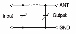
There are two different output types: Single ended and Differential. In this guide we will be designing an antenna for a Single Ended output. This means we only have one antenna trace that couples with ground. A differential output would require two antenna traces. However, a differential output can be converted to an single ended output with some passive inductors and capacitors. The below images show an example of a chip that is differential converted to single ended.
Follow the Examples
Most ICs will have a section in their datasheet which shows you a general layout, that should work. It pisses me off that they rarely include dimensions, and almost never have actual layout files. Ces’t la vie. If it was easy then everybody could be this cool.
The nRFLO1+ datasheet gives Example schematics:
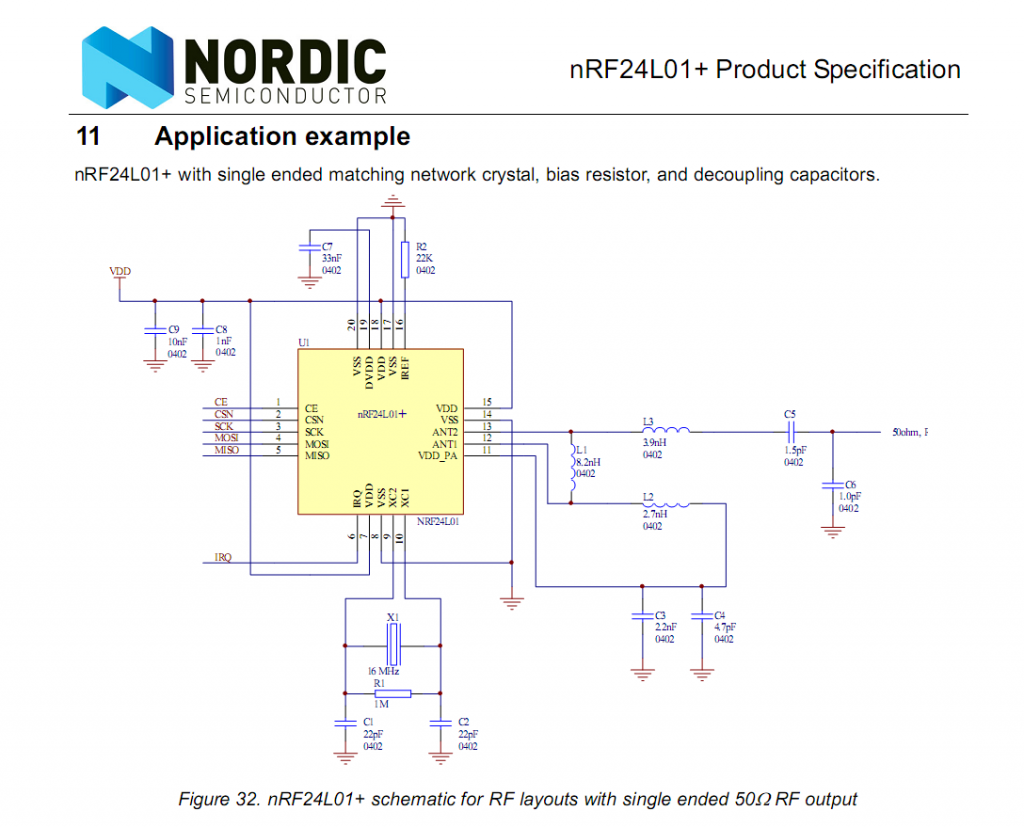
Notice that the output of the chip is actually differential but the matching components convert it to a single-ended output. Essentially this allows you to use one antenna and make things smaller. When people say ‘matching components’ they are referring to the passive parts (on the above picture, L1,L2,L3,C5,C6) that take the impedance at the chips output pin, and mash it into a nice 50 ohm output that you can match your antenna to.
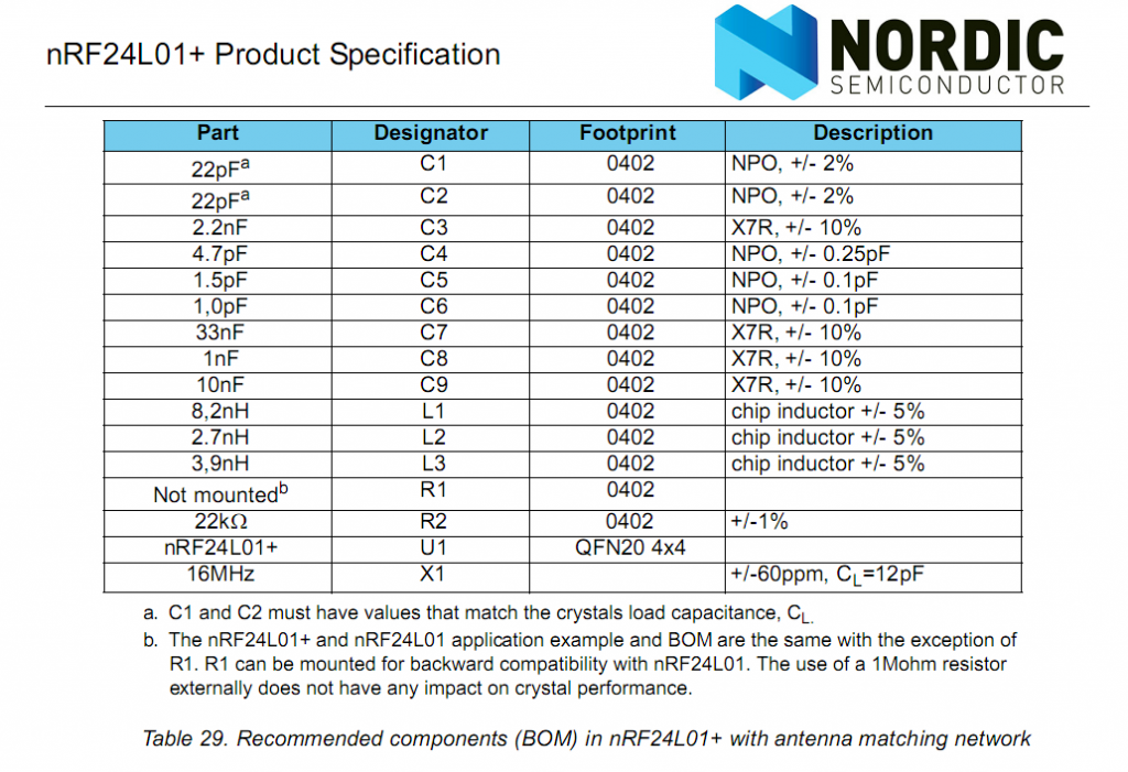
The nRFLO1+ also has an example BOM! How generous! Those kind Norwegians.
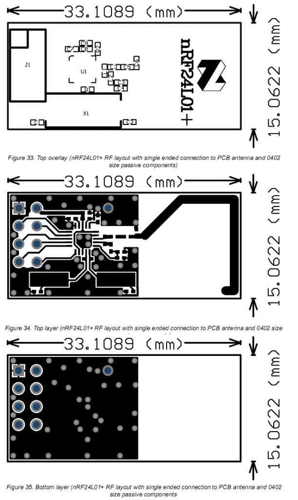
And now an example layout.
Crappy Examples
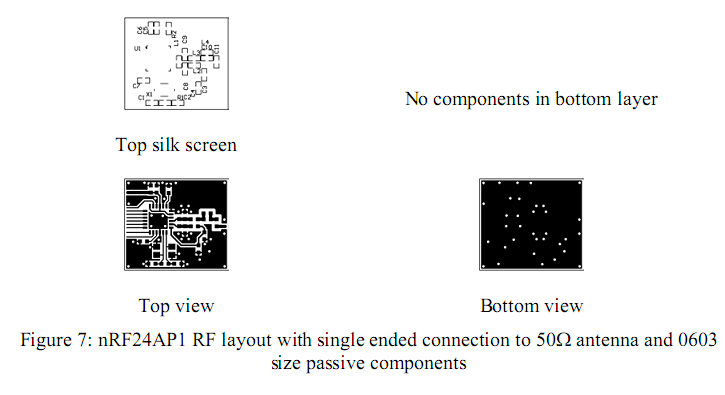
The examples vary a lot. Take for example, the example layout of Nordics nRFAP1 chip, which gives you tiny, grainy, examples and doesn’t event mention an antenna. See that little thing sticking off on the right? That’s your feedline- hook it up to an antenna. With this chip they don’t give much guidance, but we’ll figure it out.
Antenna Types
The basic options are:
- PCB Trace. The guide will cover this type of antenna.
PCB trace antennas are a good compromise between performance, repeatability, size, and cost. They are easy to tune. We will cover tuning later on.
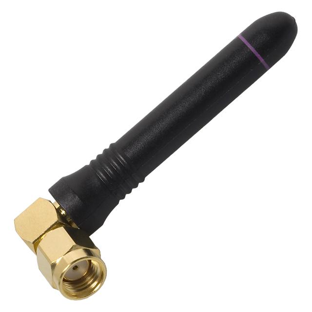
External whip antennas (also known as ducky antennas) are typically a bit larger, but are a good choice if you have the room. They are typically pre-tuned to a certain output frequency. These have good performance, the only drawback being their physical size.
Wire antennas are easy. Just cut a piece of wire to approximately the size of 1/4th the wavelength (or 5/4, or 9/4, etc) At 2.4GHz this is roughly 30mm. The downside to wire antennas? The performance will vary greatly with small changes in length and shape of the antenna. I used a wire antenna for my first wireless project and it carried about 40-50 feet under good conditions.
RF engineers seem to hate chip antennas- they work ‘for almost no apparent reason’ and can be hard to tune. From what I’ve seen, they are great in that they are tiny, but can be detuned easily. If you don’t have to transmit very far and need a tiny footprint, they’ll work fine. Make sure to include some matching components in your design so that you can tune the output. (More on this later)
Designing the Antenna
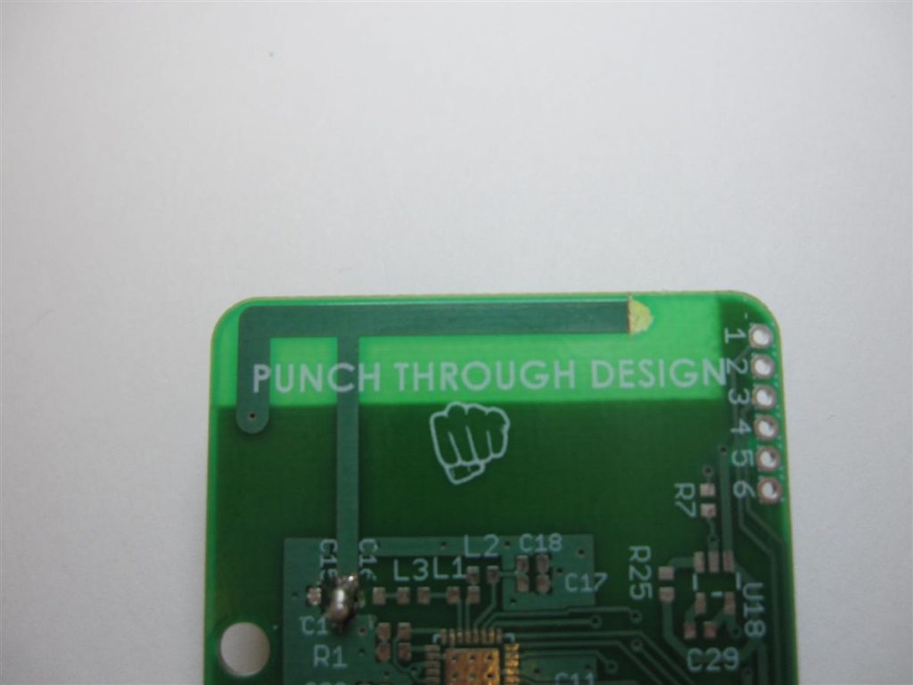
**Don’t put any ground plane beneath the tail of your F Antenna!
**Put a note on the silkscreen layer, or any other layer your Mfg will see, and tell them the antenna section of the board is sensitive to added copper! Advanced Circuits will sometimes etch an order number into the copper on your board. This will change the properties of your antenna!
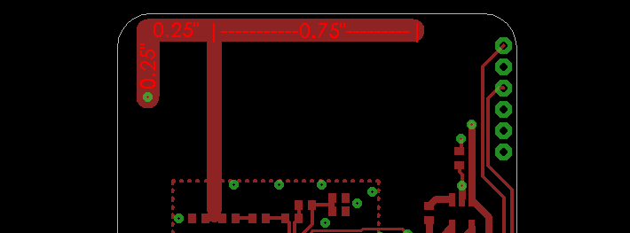
Standard Dimensions:
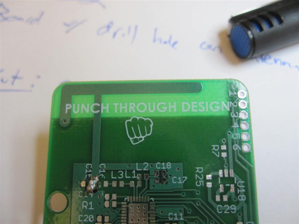
I started with an F Antenna that had a 1″ long tail, tapped 1/4″ from the left, with a 1/4″ section going to the ground plane. See the below picture for those dimensions again. The length of the feed line doesn’t really matter. The width of the feed line does. See the section further down on how to size the feedline.
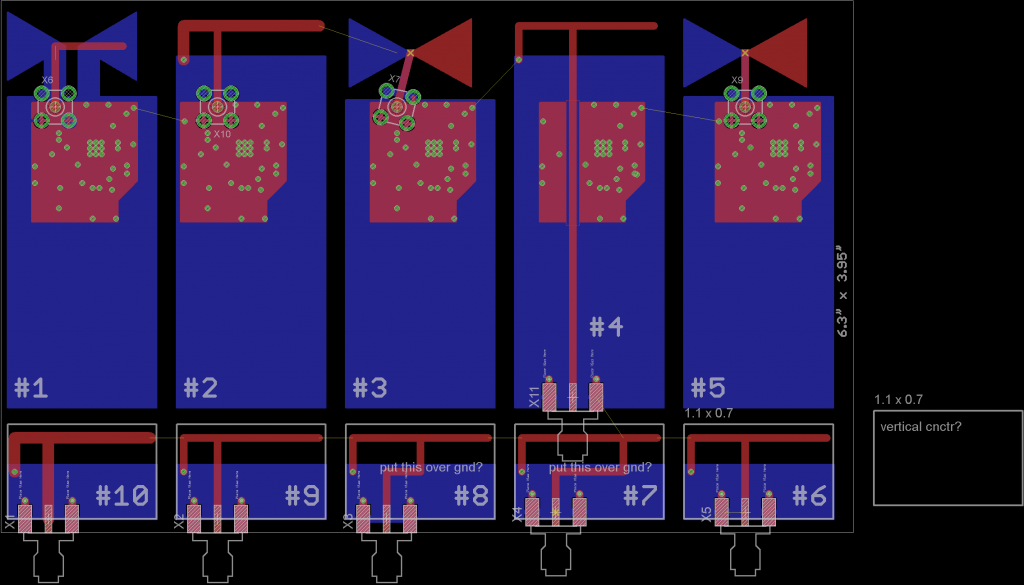
On my first antenna build, I decided to build a board with several designs on it, and then test each one and pick the top performer. However, I think you can get by with an F Antenna, and only building one.
Sizing the Feedline
The trace that connects your antenna to the output of your matching circuitry is called a feed line. You want to design this to be 50 Ohms at your desired transmit frequency. The width of the trace dictates the impedance- you can use the following link to calculate your trace width. You’ll want to use these parameters for a standard 1 oz thickness, FR4 circuit board. You can calculate other values here:
http://emclab.mst.edu/pcbtlc2/microstrip/index.html
Dialectric thickness: Typically 62 mils (0.062 inches). In my case it was 31 mils.
Trace thickness: for a 1oz thick copper PCB, usually 1.4 mils or 0.0014″.
Trace Width: Leave this blank so it calculates it.
Relative Permittivity: 4.8
Characteristic Impedance: 50
With my values, with a non-standard thickness board (31 mils thick), I arrived at 55 mils. For a standard thickness board (62 mils), it would be roughly 108 mils.
The Ultimate Rule – Impedance Matching
As a practical engineer, our biggest rule to adhere to is ‘impedance matching’. We have a chip that sends out a signal, and we want to turn that electrical signal into a wireless signal (an EM field). Our chip and antenna have characteristics that define their impedance. If those impedances are equal, or matched, we are putting as much power into the wireless signal as we can. This is known as ‘optimal power transfer’. If we aren’t perfectly matched, we will have some power loss. You can google ‘impedance matching’ for the theory behind this.
We can’t change the output impedance of the chip, but we can alter the impedance of the antenna, and we can put some parts in between the chip and the antenna, collectively forming a ‘matching network’. These parts can be used to change the impedance of the antenna so that it matches the impedance of the chip. The most common arrangement of parts is known as a Pi Network. If your example layout does not have matching components present; they do not show anything on the output pin of the chip, you will want to include these yourself. A Pi Network is shown below:
(Read this great App Note for more detailed info: http://www.ti.com/lit/an/snoa519b/snoa519b.pdf)
Tuning your Antenna
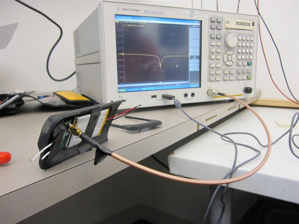
This is typically done with a network analyzer, one ridiculously expensive piece of equipment. They can be rented by the month for around a thousand bucks, but my recommendation is to make friends with someone at a local company that owns one. Or if you’re a university student, you can usually find a professor willing to let you in their lab for a little while. Another option is to find a local design firm, and ask if you can rent out their equipment per hour. Expect 100-150$/hr for the time on the equipment, and more than that if you want one of their engineers to help out. However, if you’re passionate about your project, people will usually try to help you out.
A network analyzer measures the properties of a network of components. You hook it up to your system (in our case, our antenna) and it uses a variety of techniques to determine the impedance of the network. They typically have 2 ports, although our tuning will be done with only one port, since we will be simply sending in a signal, and seeing how much power is bouncing back. We can deduce from this how much power has been converted into wireless energy.
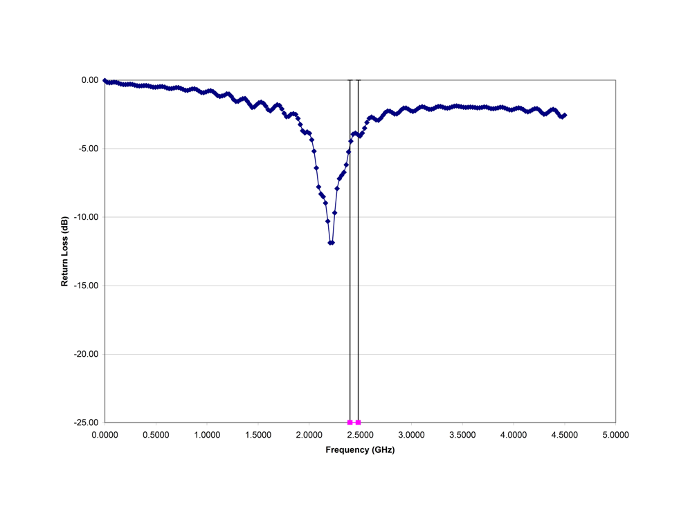
The below measurements were taken with a network analyzer. At this point we actually aren’t measuring any wireless signals, or wireless power, etc. Instead the Network Analyzer (NA) is measuring how much power is reflected by the antenna at various frequencies. If all the power is being reflected, none is being converted into EM energy. The lower the number here, the more efficient we are. At -10dB we are roughly 70% efficient. At -20dB we are 90% efficient.
So let’s get ready to tune.
Step 1, espresso:

Step 2, calibrate the NA for a one port measurement.
This is done with a calibration kit provided w/ the NA. You hook up a shorted end, an open end, and a 50 ohm end in succession. Keep in mind the shape of the cable attached will affect your results, so calibrate it with that in mind. Once you calibrate to a certain shape of the cable, test your antenna with that same shape. This is often done by taping the cable down to the table to hold shape.
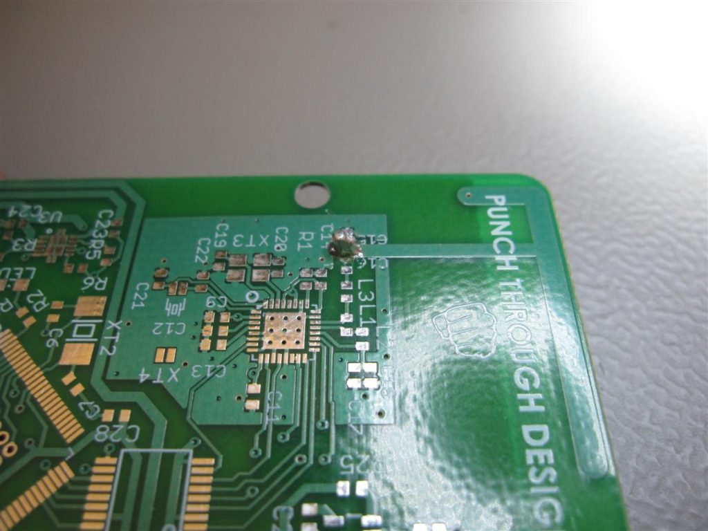
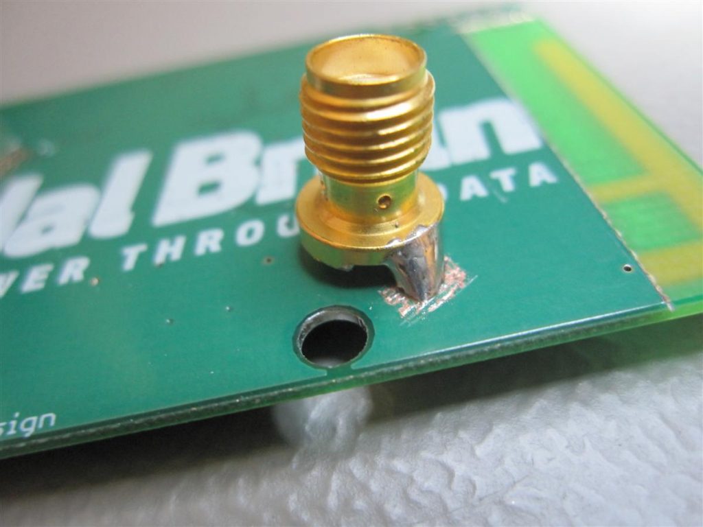
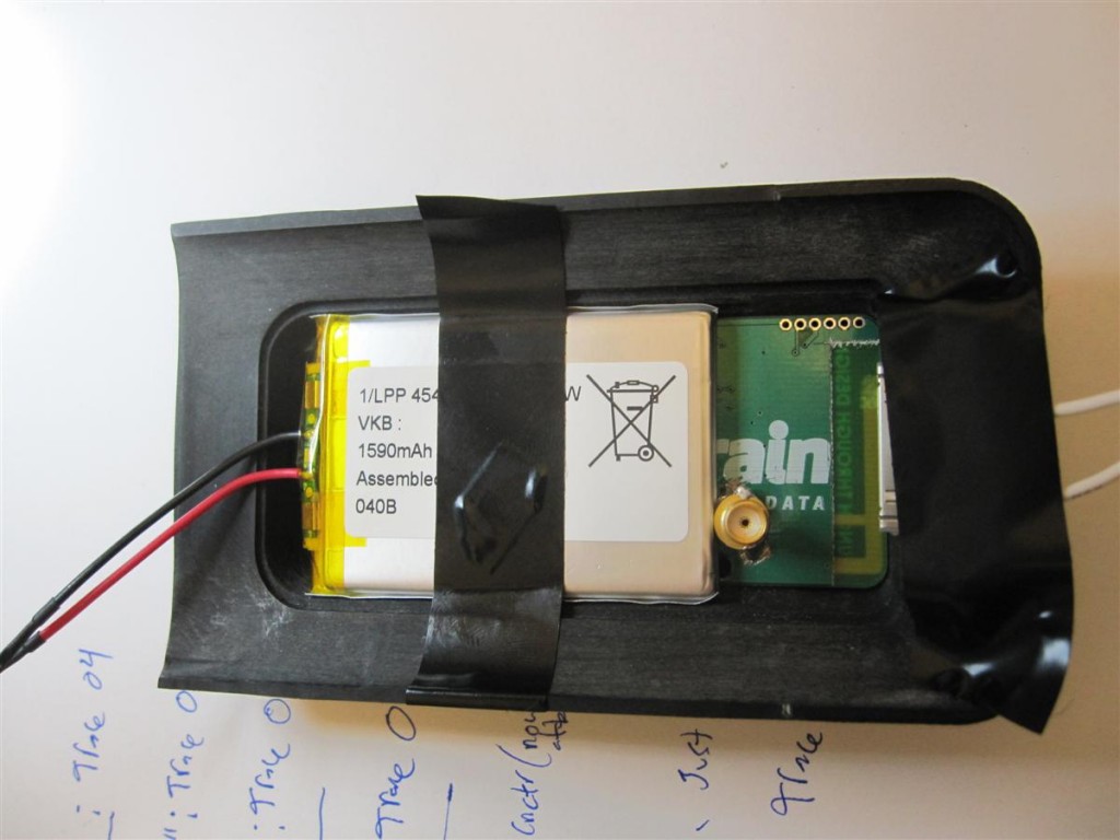
Step 3, solder an SMA connector to your antenna.
To do this I had to drill a small hole through the board where the feed line began. I then scratched off the solder mask on a small portion of the feed line, and in several places on the bottom ground plane of the board. I stuck the SMA connector through the hole and soldered it up.
An Edge Mount SMA connector- J657-ND
Vertical Mount SMA connector- J500-ND
Step 4: Hook it up, start hacking away
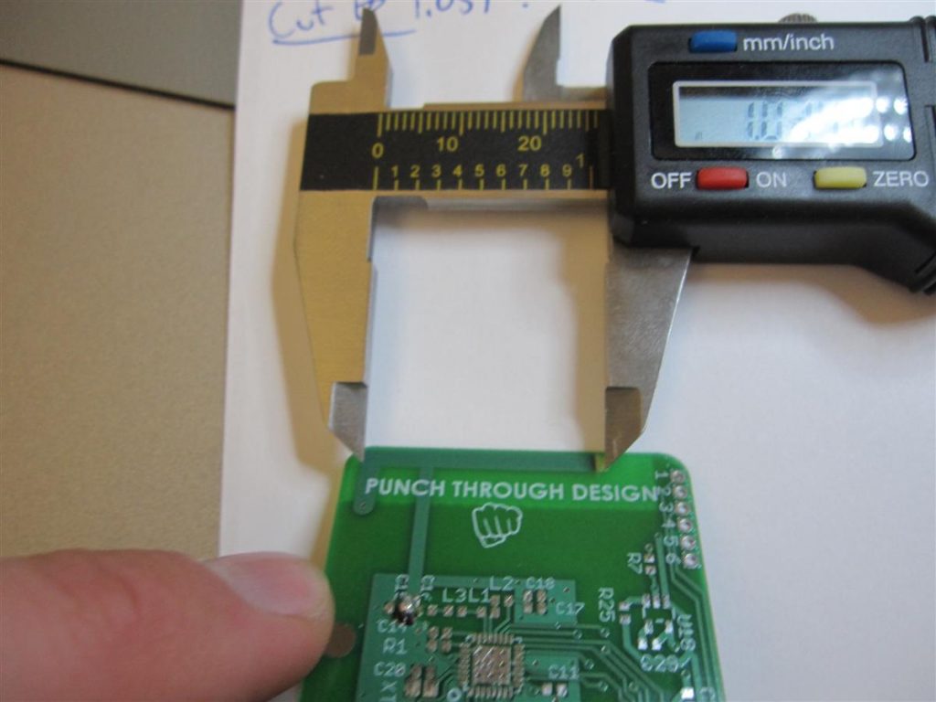
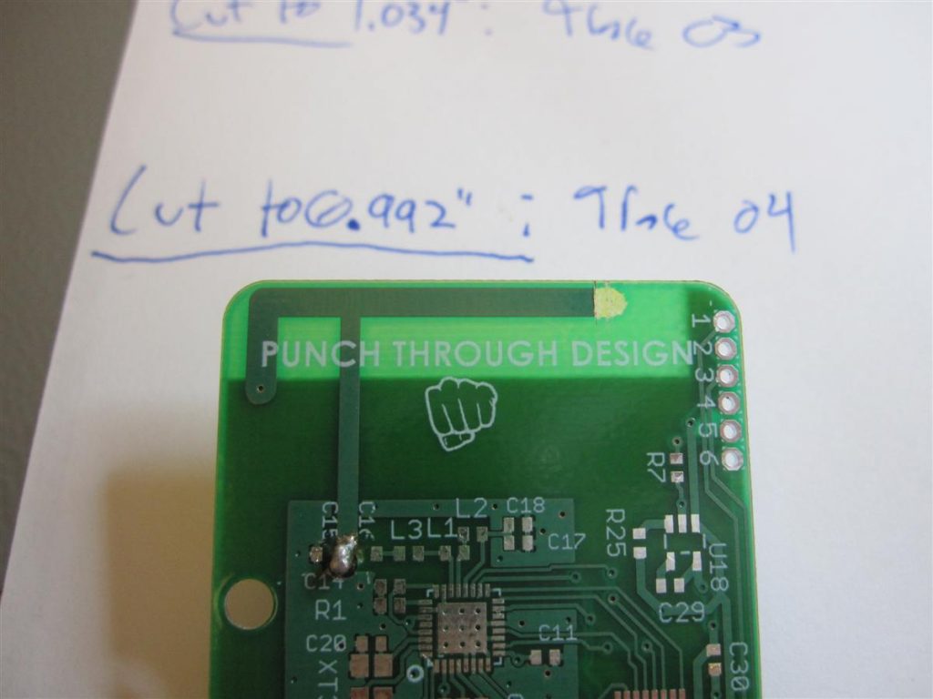
PCB Trace Antennas, more specifically the F-Antenna (also called PIFA), is a simple antenna to tune. Everything can be done by varying the length of the tail. This is accomplished by slicing your antenna to various lengths with an exacto knife. Don’t you love working on hardware? If you think about it, it makes total sense. If you make the antenna shorter, your resonant frequency will have a shorter wavelength, and therefore a higher frequency. So cutting your antenna shifts it up in frequency. This is why you want to design your antenna long to begin with, since it’s much easier to cut it than to add on to it. If you do have to go down in frequency, you can actually add copper tape, although the barrier between your PCB trace and the copper tape will often throw off your results. Rule of thumb, on your first design, make the antenna a bit longer than it needs to be. Then you can try different sizes easily.
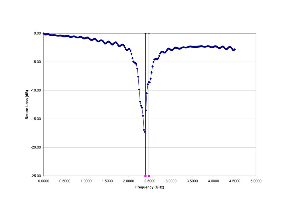
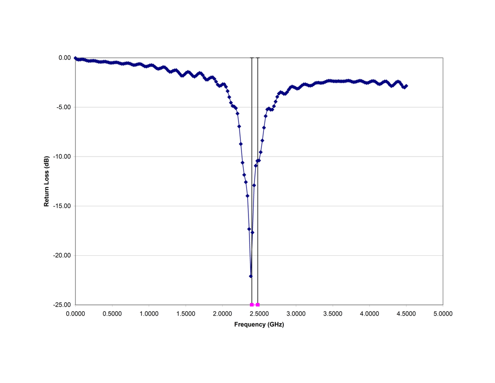
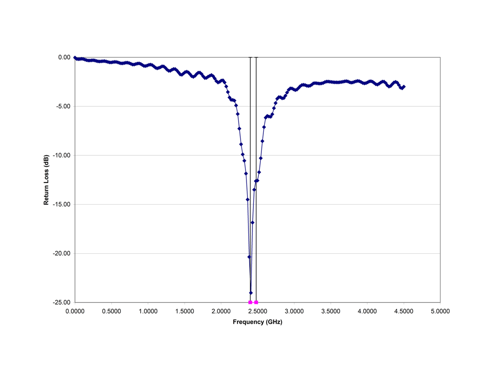
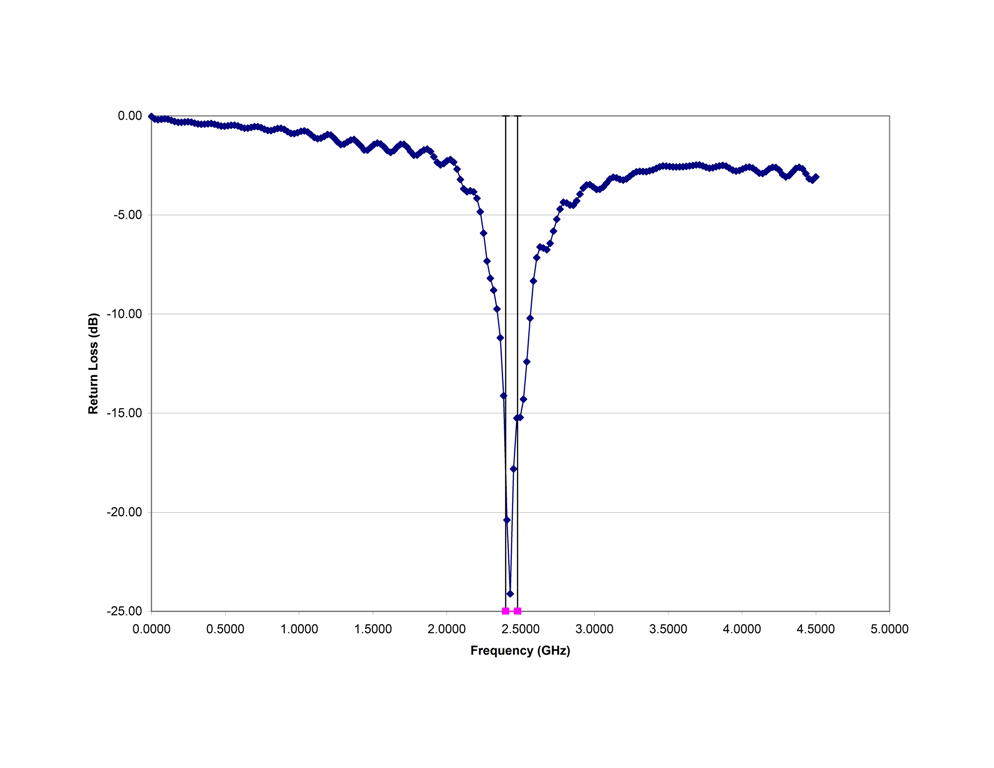
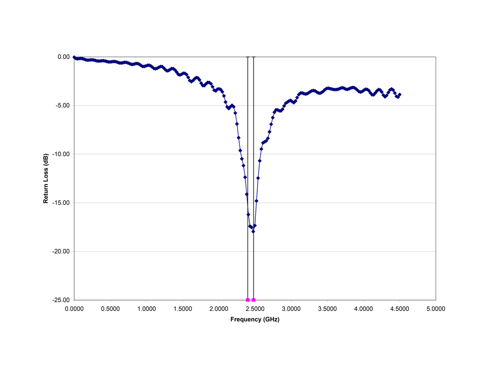
On the plots, the vertical lines represent the band we are operating in. Ideally we want the trough close to our center frequency, 2.45GHz.
First measurement, with the full antenna:
Second measurement:
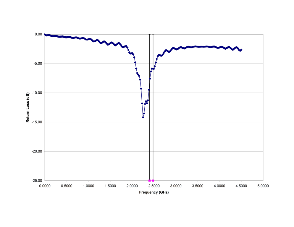
Third measurement
Fourth:
Fifth:
Sixth:
Important thing to remember- everything surrounding your antenna will affect the performance. This means your case, battery, wires, connectors, a user’s hand, etc. The trace above and below are measured with the same exact size of antenna, but the trace below has a plastic case and battery in place. Notice the difference:
Seventh:
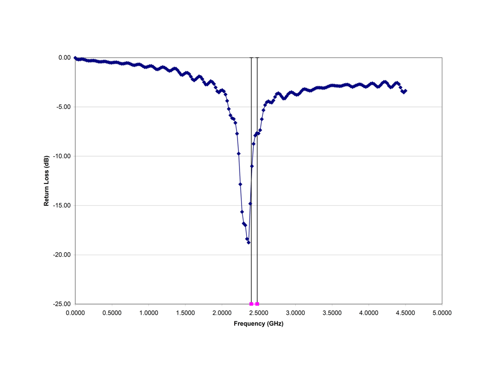
Finally, the eight and final measurement. Close enough to be happy.
Smith Charts
Power loss is one way to look at our antenna, but another common method to visualize the parameters of an antenna is called a Smith Chart. Here is an example of a big scary looking smith chart:
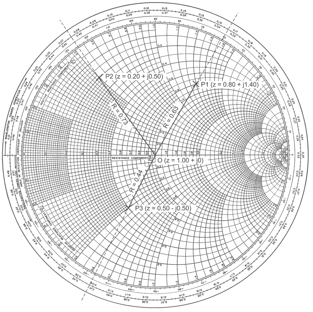
Basically a smith chart is a convenient way to picture real and complex impedances on one graph. Note that the impedances are normalized, typically to 50 ohms. This means that your true impedance is found by multiplying the magnitudes on the chart by 50. Every network of components has a real and complex characteristics which define their impedance. The real part of the impedance is noted by the expanding circles, whose diameter is noted along the horizontal line in the middle of the smith chart. The imaginary part is noted by the lines that bend away from the horizontal line. Together, where they intersect, forms a point on the smith chart which represents the impedance. The top half of the smith chart represents an inductive impedance and the bottom half represents a capacitive impedance.
A network analyzer can display a smith chart as well as the power loss we did before. We are shooting for 50 ohms impedance, but chances are we will be a bit off. The below image (from a National Semi app note) shows how to get closer to 50 ohms by changing values of the matching components we added before:
From what I’ve seen, if your chip’s datasheet has a good section on your example layout, and gives you values for matching components, you probably won’t need to worry about smith charts. So all is not lost if none of this makes sense. However, smith charts will help you fully understand what is happening.
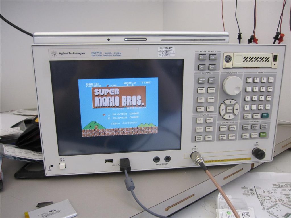
Hooray! We’re done. Everyone’s happy. Reward yourself with a little network analyzer Mario:
FCC/CE Testing
If you’re going to make more than a few (I believe the official number is 5) of your design, you will have to get FCC (or CE for Europe) certified or your device can be taken off the market. If you plan on only making small batches, using a wireless module that is already FCC certified might be a better solution.
My most recent design for PedalBrain was FCC and CE certified without any major problems. There were hiccups along the way, but we were able to bring the output power down a bit to pass the tests. This is, however, an expensive exercise, so do your best to avoid it.
Email me if you use this guide, I would be happy to see what you come up with. Also email with questions if you run into problems. You can reach me at my first name DOT my last name (hint, they are in the domain) @gmail.com
Now go build some stuff!

Is this why some cellphones have an antenna connector at their back?
Thank you so much for posting this great methodology! I don’t feel dirty at all as long as the job’s done!
A few suggestions (from an RF guy):
1. If you use a reference antenna design provided by an IC manufacturer, make sure that you know what PCB material and thickness they used in their design. Duplicate it precisely in your design. Even the position of vias around the antenna and the thickness of the copper layers (1 oz vs 2 oz) can make a difference, but if you match the material and overall thickness you should be ok. Watch out for multilayer boards where they use L2 instead of L4 as a groundplane, I have seen lots of this kind of stuff. Also keep in mind that the guy who made the app ckt for the IC may not be a very good antenna designer, so YMMV. 🙂
2. I use AppCAD to calculate microstrip trace widths.
http://www.hp.woodshot.com/
3. Tuning an antenna (or changing the matching network that feeds it) can affect the performance of the antenna in terms of gain and directivity. Just because it is a good match doesn’t mean that you haven’t thrown away some other performance parameter of the antenna. Some great antennas can have crappy impedance matches.
4. Testing an antenna on a network analyzer is tricky business, especially if you are in an enclosed room with other objects in it. Try to at least keep the antenna a few feet away from any large metal objects, and note how much the impedance changes as a function of orientation. However, I have done exactly what you did with good results for amateur radio antennas, so it can work!
5. The FCC has all sorts of rules regarding power output (ERP) and spurious emissions for most frequency bands, including 2.4GHz. By designing a custom antenna and PCB layout for an RF chip, I think you are now supposed to have your device tested and certified by the FCC before you can actually sell it. This is why usually hobbyists and small companies will just buy pre-certified RF modules (like the Xbee). Since the module is already certified, you don’t need to worry about the FCC unless you change something about the module design (ie. adding an external antenna). I don’t know the specifics but it would be best to check the rules before going to market (or perhaps you already have plans to get your design certified).
Thanks for all the info! I’ll check out your method for feed line calculations.
Regarding FCC testing- this design has already been FCC and CE certified. That was an interesting process as well and probably deserves its own blog post. We were able to pass with only minor corrections and dropping the tx power a couple notches.
Great post! As a cell phone design engineer, I enjoyed reading it. Nice to see mightyohm here too, I read his blog. AppCad is a great and free tool from Agilent. I used to work with the author actually.
Regarding pp6’s question, that connector is used for testing and calibrating the phone in the factory, as well as in the certification labs (FCC and other industry certifications that are needed).
Excellent article for the practical streetsmart designer!!
An interesting read, do you think you could do an article on getting the fcc/ce testing? I can’t think of any good guides to getting it or the costs involved and it would be nice to hear from someone with firsthand experience.
Thanks for those advice.
Usually, CE lab guy say “CE+CE doesn’t equal CE” so, buying an already CE
certified (R&TTE + ETSI 300440 …) RF module may not get rid of the lab certification process for your product including it.
I have read a little about fractal antenna’s. I am sure they are more difficult to design. But are there some DIY pointers about them somewhere? I’ve been looking, but probably in the wrong places.
Nice article. I had to do an antenna for a 413MHz design a year or 2 back and at the time had no experience with the tools you described above. All I could do in that case was to design the antenna longer as you suggested and watched an RSSI reading at the other end as I tuned the antenna by moving my finger along the length of the antenna until I got a good strong reading. From that point i could fine tune by cutting the antenna at around that point. Def not recommended for FCC approval though!
Its nice article. this the best . I am sure they are more design. keep a good works..
Great stuff. I’ve just spotted this guide from TI which is handy too:
http://focus.ti.com/lit/an/swra161b/swra161b.pdf
Colin – This is a really great article. Here are my additions. You might want to pull back the solder mask from the antenna to avoid some of the mask losses you might incur at 2.4GHz. When using the network analyzer, you will want to use ferrite beads to isolate the antenna from the analyzer. This will prevent RF currents from circulating on the coax ground connection.
well done , we design gsm and 3G and have been doing design for 10 years
some of the pcb antenna we purchase are not much chop
We are in the process of starting to design our own ,and unforntuntaly i will have to get my head in the books again, your site make my life just that better , hey well done